4-bit alu design in verilog using xilinx simulator
Testbench VHDL Code for 4-Bit ALU. Its a basic block in any processor.
Vhdl Code For 4 Bit Alu
Go to line L.

. Electrical Engineering questions and answers. Always S A B begin case S 2b00. D and need your support to solve the warnings messages on my code below.
3 Sri Venkateswara Engineering College. There are 6 different functions implemented in this ALU. Open 3264-bit Project Navigator.
Verilog code for Clock divider on FPGA. Design methodology has been changing from schematic design to HDL based design. Mihir Gajjar and Mihir Gajjar 4 - bit ALU using Verilog.
This commit does not belong to any branch on this repository and may belong to a fork outside of the repository. Table of 32-bit Arithmetic Logic Unit 31. ALUArithmetic Logic Unit is a digital circuit which does arithmetic and logical operations.
Department of Electronics and Communication Engineering Athihrii Stephen Sanjay 2016 Page 19 Design and implementation of 32-bit ALU using Verilog 2016 Fig34 Arithmetic Logic Unit 32. 4 - bit ALU using Verilog. RTL design starting from designing a top level RTL module for 4-bit ALU using hardware description language VHDL.
Module LU input 10S input A B output reg f. The result is denoted by R which is also 8 bit long. Code 011 5 4 input NOR operation using dynamic NOR gate op.
The codes are simulated in Xilinx ISE 131 to get the following waveform. For shifter unit the selection line S1 is used to select either left or right shift micro-operation. To a chieve a successful ALU d esign we.
Include addition subtraction and shifting We proposed arithmetic and logic unit using VHDL structural and dataflow level design. We put up with this kind of Verilog Simulation graphic could possibly be the most trending topic gone we share it in google pro or facebook. Assign S ABCIN.
The input signal Op is a 3 bit value which tells the ALU what. Cannot retrieve contributors at. The arithmetic logic and shift units can be combined into ALU with common selection.
An Arithmetic logic unit system has been developed by sequence of operations and. INTRODUCTION A 64-bit ALU implemented using VHDL and verified on Xilinx ISE simulator. This research paper is based on the simulation of 16 bit ALU using VHDL.
I am supposed to create 4 bit full adder verilog code in vivadoBut when I try to test in the simulationIt give me z and x outputWhich part of code I have to change to get an output in simulation. N-bit Adder Design in Verilog 31. The design was implemented using VHDL Xilinx Synthesis tool ISE and targeted for Spartan device.
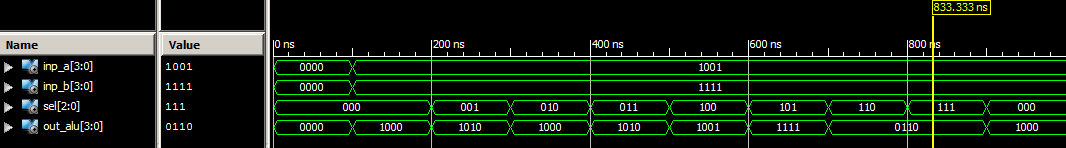
Ac89774 on Mar 29 2017. Explain by Examples 32. Simulation Result for 4-bit ALU.
You can uncheck Show Tips at Startup if you do not want the. We proposed arithmetic and logic unit using VHDL structural and dataflow level design. Design methodology has been changing from schematic design to HDL based design.
F A. AIM The main aim of this project is to design and simulation of different 8-bit multipliers using VERILOG code Considering their advantages and disadvantages these are compared on the basis of area speed and delay. Code 000 2 2s Complement of A op.
This video describes the complete simulation flow step by step for VHDL Code using Xilinx ISE Design Suite 147 It helps beginners to understand the working. Up to 24 cash back N-bit Adder Design in Verilog. This paper presents design concept of 4-bit arithmetic and logic unit ALU.
Code 010 4 4 input NAND operation using static NAND gate op. On the other hand when M1 the output of the 4-bit ALU is a 2s. Go to file.
The approach used here is to split the ALU into three modules one Arithmetic one Logic and one Shift module. Verification of the designed RTL code using simulation techniques synthesis of RTL code to obtain gate level netlist using Xilinx ISE tool and Arithmetic Logic Unit was successfully designed and. Full VHDL code for the ALU was presented.
Code 001 3 4 bit Add-traction op. Assign COUT A. It can be used in integer arithmetic computations and as Complex operation.
Verilog Simulation - 19 images - system verilog tutorial vhdl delay timer ls7212 in verilog hdl design flow and methodology system verilog tutorial vhdl. All the modules in arithmetic and. Functional Description of 4-bit Arithmetic Logic Unit.
Digital Clock manager DCM in Xilinx FPGA. An ALU performs following operations Addition subtraction multiplication Not logical shift. This paper presents design concept of 4-bit arithmetic and logic unit ALU.
In this Video you will learn how to design or implement the 4 bit ALU in verilog using Xilinx Simulator in very simple waySee Code here httpwww2dixco. Im working on a project to implement 4-bit ALU using four 1-bit ALU using Xilinx Verilog code on my Real Digital Blackboard rev. Module my_full_adder input A input B input CIN output S output COUT.
When M0 and the result from the 4-bit ALU is Logic based the result is displayed on an array of LEDs. Code 100 6 1s Complement of B op. Go to file T.
As you can see it receives two input operands A and B which are 8 bits long. For this tutorial we have Xilinx ISE 144. 1 4 bit Addition op.
Since the output of the 4-bit ALU F30 is dependant on the signal M we have two ways of displaying our results. Click OK to close the Tip of the Day window that pops up. Each module of ALU is divided into smaller modules.
The testbench Verilog code for the ALU is also provided for simulation. RTLRegister Transistor View Shift Unit VHDL. Controlled by the three function select inputs sel 2 to 0 ALU can perform all the 8 possible logic operations.
Each module of ALU is divided into smaller modules. Execute was to design a 1-bit ALU and then combine four of them to create a 4-bit ALU. Make sure you have installed Xilinx ISE 144 or later.
Follow the below-mentioned procedure to simulate your first Verilog program. The block diagram of the ALU is given below. Last time an Arithmetic Logic Unit ALU is designed and implemented in VHDL.
4 bit ALU Design in verilog using Xilinx.